STM32 GPIO Registers
- Port Direction Registers
- Port Speed Registers
- to decide the slew rate of the GPIO. Low Speed, Medium Speed, High Speed and Very High Speed modes available
- Port Output Type Register
- Port Output Data Register
- Port Input Data Register
- During Read value of GPIO, the data will be updated every AHB1 Clock Cycle
- GPIO Port Pull Up and Pull Down Registers
- Some Other configuration registers
All the GPIO Registers are connected to the Processor over the System Bus. AHB1 Bus and frequency depends on the Controller.
And GPIO Ports n depends on the Controller it can vary based on the controller to controller in the Same STM32 itself.
Each Peripherals having the Register section in the user manual. There we can find the register related info.
GPIO PORT MODE Register (GPIOx_MODER)
This GPIO PORT Registers is 32Bit Registers and all the Ports in the Controller having PORT MODE Registers
x – PORT
Things to be considered during Setting of PORT MODE Registers
- Address OFFSET: Indicates how much offset from the GPIO PORT Mode Register Address
- Base Address + OFFSET is the address which is correspond to Port MODE
- Reset Values: On Reset the mentioned value will be available to the particular register later during Init desired values needs to be set by ourself
- Types of Modes
- Input Mode (Also can be used as Interrupt)
- General Purpose Output Mode
- Alternate Function Mode
- Analog Mode
- GPIO Supporting Mode will be mentioned in the datasheet, it will vary GPIO to GPIO.
Before Using any GPIO, must define the MODE. Whether wanted to use its above mentioned MODE.
Structure of Input and Output Port
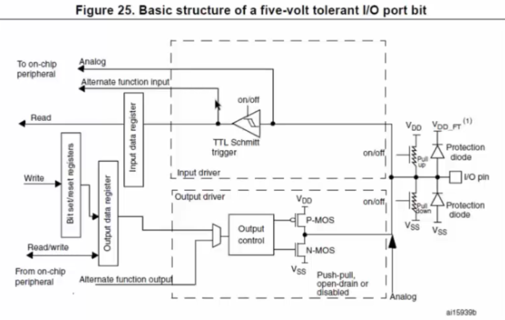
Input Mode Configuration
- During Input Mode, Output Driver will be fully disabled
- Input Data Register will read the I/O Pin state on every clock cycles.
- Remember, All the GPIO is connected to the AHB1 Bus Directly. So Every AHB1 Cycles state of the I/O Pin will be read and stored in the Input Data Register.
- Default Pull up and Pull down configuration will be disabled, in SW it has to be enabled
- Pull Up or Pull Down configuration is very good to avoid Noise from the Output Driver though it is disabled and during this time, Without Pull up or Pull down. This input will be called as Floating Input
- To avoid noise from the input pin, pull up and pull down resistor will help
- We can use external pull up or pull down resistor or using configuration we can also use internal pull up or pull down resistor. Recent modern microcontroller comes with internal pullup resistors.
- These values of the internal Pull up and Pull resistor will be available in the section
- weak pull-up or weak pull-down section of I/O Static characteristics
- weak pullup or pulldown means in electronics, there is a higher resistance value available and which allows only less current.
- In some scenario such as any design limitation where power or delay in power fail or impedence or any kind of delay needed or any functional requirement is specially needed to provide the specific value of resistor then in that case. External Pull up is required or else we can go with internal pullup
Output Mode Configuration
There are two Output Mode Configuration available
- Push Pull (Pull Up
- Open-Drain
Push Pull Configuration (refer the above diagram for understanding below points)
- Here, Input Driver is not disabled. Input driver also ON. During Output we can still read so that Input driver will be activated
- Output Description of Value ‘0’
- When we write 1 to Output Data register. Then In Output Control assume there will be NOT Gate connection present. When we Pass to output control output value 0’1′ and PMOS will be enabled and LED connected to the GPIO is enabled
- when we write 0 to Output Data register. Output Control is NOT Gate -> ‘1’ —> PMOS Deactivated and NMOS Activated —> Pulled to GND and State of GPIO is LOW and
Open-Drain Configuration
Alternate Function Configuration
- Here, when we need to use the GPIO for some peripheral configurations such as UART, I2C and SPI then Alternate function can be used.
- During this configuration
- Output Control is driven by Alternate Function Output, Eg: UART Tx or SPI MOSI
- Input Driver is driven by Alternate Function Input. Eg: UART Rx or SPI MISO etc. also Here Input data register will be still enabled though we can read the data from the PIN.
- So technically, for input both alternate function input and input data register also.
- When GPIO is in Alternate Functionality mode, it can be used for 16 different functionalities
- AF0 to AF15; refer datasheet (alternate function map) for more information (not usermanual)
- There will be register for Alternate function selection for GPIO when choosing alternate function
- GPIO Alternate function Low register (AFRL0 to AFRL7) Alternate function Register Low
- Pin # 0 to 7
- GPIO Alternate function High register (AFRH0 to AFRH7) Alternate Function Register High
- Pin # 8 to 15
- For example if PA0 as UART4_TX configuration then GPIOA_AFRL0 can be used to select the corresponding AFx here AF8 is for UART4_TX.
- GPIO Alternate function Low register (AFRL0 to AFRL7) Alternate function Register Low
Clock Enable
To Enable GPIO working, Clock Source has to be enabled.
RCC Module is responsible for Clock Setting. We can Enable RCC_AHB1ENR register to enable and disable